

IBM makes circuits on graphene, a razor-thin revolutionary material
A research team at IBM has made a circuit from graphene, a razor-thin revolutionary material. This marks a significant milestone in the use of graphene in practical devices, which could one day replace many uses of the ubiquitous silicon.
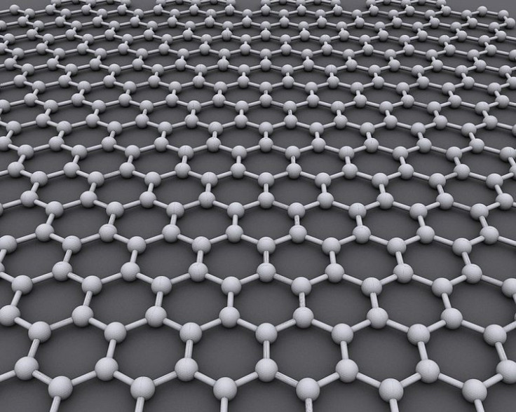
Graphene is essentially a 2-dimensionsed sheet of carbon atom lattice (pictured left). (It’s deemed 2-dimensional because it is only one atom thick, whereas the thickness of most materials are at least several atoms).
It’s potentially more attractive that silicon and other materials because it’s thin (good for nanotechnology), has excellent electrical conductivity (faster than silicon), could be very low cost and widely available once extraction technology advances, and could allow for more control and predictability due to its two dimensional structure.
Previously, researchers had trouble using graphene to essentially replace other materials in the construction of widely-used electrical equipment. What the team at IBM did was use it to create an integrated circuit.
Moreover, it did so “using existing manufacturing techniques, suggesting their designs could be affordable enough to commercialize,” according to MIT’s technology review.
Integrated circuits are widely used in wireless communication. If graphene becomes prevalent in that area, it could become one of the most important materials in technology and potentially rival the dominance of silicon.
© Copyright IBTimes 2024. All rights reserved.
-

Microsoft Expands Its AI Empire Abroad
-

Oil: 'Mother Of Corruption' In Venezuela
-

'Extreme' Climate Blamed For World's Worst Wine Harvest In 62 Years
-

Macron Warns 'Mortal' Europe Needs Credible Defence
-

Bitcoin And Crypto Price Review - Another Myth Gets Busted?
-

Mass Cancellations Loom Despite French Air Union Cancelling Strike
-

Mired In Crisis, Boeing Reports Another Loss
-

Recycled 'Zombie' Misinformation Targets US Voters
-

Hackers Leak Part Of Source Code Of El Salvador's Bitcoin Wallet
-

Azerbaijan Says 'Closer Than Ever' To Armenia Peace Deal Amid Border Talks


