Artificial Graphene Created On A Semiconductor Device Using Nanofabrication Techniques
In an important breakthrough in physics and materials science, researchers have for the first time engineered artificial graphene in a semiconductor device.
Columbia University School of Engineering and Applied Science researchers worked with colleagues from Princeton and Purdue Universities and Istituto Italiano di Tecnologia to achieve the milestone.
By intricately manipulating matter on a nanoscale, the team etched the unique 2D electronic structure of graphene onto a semiconductor material called gallium arsenide.
Artificial graphene has already been demonstrated in other systems such as optical, molecular, and photonic lattices but the semiconductor breakthrough offers more possibilities to modulate electronic behavior.
"This milestone defines a new state-of-the-art in condensed matter science and nanofabrication," says Aron Pinczuk, professor of applied physics and physics at Columbia Engineering and senior author of the study in a press release on EurekAlert
"Semiconductor artificial graphene devices could be platforms to explore new types of electronic switches, transistors with superior properties, and even, perhaps, new ways of storing information based on exotic quantum mechanical states," he added.
Electrons in graphene behave like particles that move close to the speed of light, giving them unique properties that electrons in other conductors do not possess.
Since its discovery, scientists have constantly tried to figure out ways in which graphene could better existing technology and open up a whole new realm of superior tech. Graphene's 2D state and unique atomic arrangement of carbon atoms gives researchers a platform for testing new quantum phenomena that are difficult to observe in conventional material systems.
Graphene has immense electronic potential. It is the most conductive material ever discovered and forms the perfect barrier which does not allow even helium gas to pass through it. It is 200 times stronger than steel and transparent, all while being thinner than human hair. Almost every industry in the world would benefit from exploring the potential of graphene, and etching a modified version of it onto a semiconductor zaps the electronic, communication and data storage potential of this material to whole new heights.
The structure of graphene is rigid. The position of the atoms in the lattice is always fixed. This offers some experimental restrictions. But, the lattice can be engineered over a wide range of spacings and configurations. This property gives it its versatility.
With artificial graphene, researchers can modify the honeycomb lattice to modulate electronic behavior.
Because the spacing between the quantum dots in artificial graphene is much larger than the inter-atomic spacing in natural graphene, researchers can observe more exotic quantum phenomena with the application of a magnetic field on it.
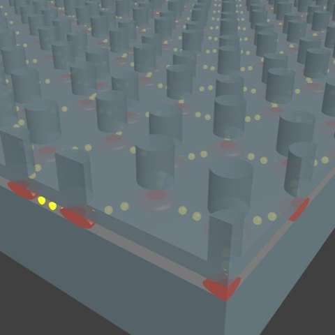
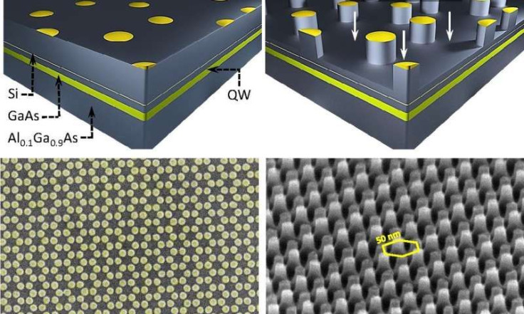
The team used an existing process, developed by Columbia engineers, which involves using patterned 2D electron gas to induce electronic properties in the artificially created lattices on the semiconductor. The researchers used conventional chip designing technology to create the lattices.
The layered structure created a narrow path for electrons to move. Using nanolithography, a pattern was created so that electrons were confined in the lateral direction in the hexagonal lattice.
By using quantum dots placed less than 50 nanometers apart, the team induced quantum mechanical interactions in the lattice, similar to the way atoms share their electrons in solids.
The team used laser light to probe the electronic lattices in the structure and measured the light that was scattered, which helped prove the graphene like electronic property.
“The scattered light showed a loss of energy that corresponded to transitions in the electron energy from one state to another. When they mapped these transitions, the team found that they were approaching zero in a linear fashion around what is called the "Dirac point" where the electron density vanishes, a hallmark of graphene,” said study, which was published in journal Nature Nanotehcnology.
© Copyright IBTimes 2026. All rights reserved.
- MOST POPULAR IN Technology