

Making Pristine Graphene Without Wrinkles For More Efficient Devices
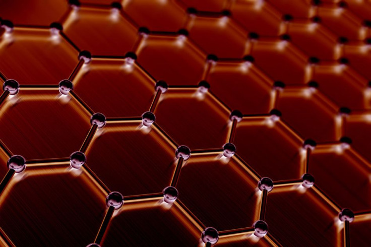
So far as unusual materials go, graphene is quite outstanding — it is among the strongest, lightest and best conducting materials known to humans. And at only one atom wide, it is also the thinnest, effectively a 2D material.
However, the unique electrical properties of this carbon variant (such as the fact that electrons travel in it at almost the speed of light) are somewhat tempered by physical imperfections in the surface, caused by the usual method used for its fabrication. But a team of researchers has developed a new method to produce graphene that smoothens the wrinkles on its surface, potentially enabling much faster and more efficient electronic and photonic devices in the future.
Read: MIT Scientists Create Porous, 3D Graphene
A paper published Monday in the Proceedings of the National Academy of Sciences describes the new method developed by scientists from Massachusetts Institute of Technology (MIT), University of California at Los Angeles, Kyungpook National University in South Korea and researchers from IBM. Titled “Unveiling the carrier transport mechanism in epitaxial graphene for forming wafer-scale, single-domain graphene,” the paper said using the new process created “single-domain” graphene which had both uniform atomic arrangement and electronic performance.
The imperfections, or wrinkles, on the surface “can derail an electron’s bullet-train journey, significantly limiting graphene’s electrical performance,” read a statement Monday on the MIT website.
Using a process called layer-resolved graphene transfer, researchers peeled off the topmost graphene layer from a silicon carbide wafer using a thin sheet of nickel. This creates step-like wrinkles on the surface that can be up to several nanometers in size, compared to the most common method — called chemical vapor deposition — wherein the wrinkles are several microns in size.
The small wrinkles created in the LRGT method are smoothened out by oxidizing the silicon wafer onto which the graphene is to be transferred. The silicon dioxide so produced pulled the carbon atoms from the graphene onto the wafer, flattening all the wrinkles. This would not work on wrinkles that are several microns in size.
Jeehwan Kim of MIT, lead author of the paper, said in the statement: “For graphene to play as a main semiconductor material for industry, it has to be single-domain, so that if you make millions of devices on it, the performance of the devices is the same in any location. Now we can really produce single-domain graphene at wafer scale.”
The potential uses for graphene are numerous and varied, from electronics to transport, medical devices to to sporting equipment, and even for environmental protection. A speculative list can be seen here on the 911Metallurgist website.
© Copyright IBTimes 2024. All rights reserved.
-

Bitcoin And Crypto Price Review - Another Myth Gets Busted?
-

Mass Cancellations Loom Despite French Air Union Cancelling Strike
-

Mired In Crisis, Boeing Reports Another Loss
-

Recycled 'Zombie' Misinformation Targets US Voters
-

Hackers Leak Part Of Source Code Of El Salvador's Bitcoin Wallet
-

Azerbaijan Says 'Closer Than Ever' To Armenia Peace Deal Amid Border Talks
-

How UK's Biggest Water Supplier Sank Into Crisis
-

Taiwan Hit By Dozens Of Strong Aftershocks From Deadly Quake
-

Gaza Health System 'Completely Obliterated': UN Expert
-

In Ecuadoran Amazon, Butterflies Provide A Gauge Of Climate Change


