

Scientists Determine 3D Position Of Individual Atoms For First Time
Scientists from the University of California, Los Angeles, (UCLA) said Monday they were able to pinpoint the dimensions and locations of individual atoms and their positions within a structure for the first time.
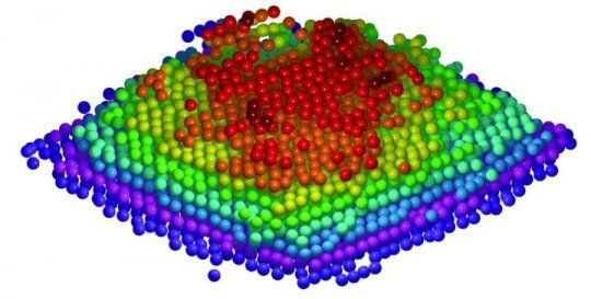
Researchers said that they used a powerful microscope to identify the three-dimensional positions of individual atoms to within 19 trillionths of a meter, several times smaller than a hydrogen atom. The result of their research was published in the journal Nature Materials.
The findings also make it possible to study the macroscopic properties of materials by closely examining their atomic structure, which could, in turn, help in the construction of aircraft components and other advanced materials, the scientists said.
Previously, scientists had inferred the position of atoms in 3D structures using a technique called X-ray crystallography, which used measurements of light scattering off crystals. However, the method only yields information about the average positions of many billions of atoms in a crystalline structure, and not the individual atoms’ precise coordinates.
"It's like taking an average of people on Earth," research lead Jianwei Miao, professor of physics and astronomy at UCLA, said in a press release. "Most people have a head, two eyes, a nose and two ears. But an image of the average person will still look different from you and me."
This means that X-ray crystallography would not be able to identify weaknesses such as the absence of a single atom in a structure. These weaknesses, known as point defects, can severely diminish the overall strength of a structure, which could be dangerous in machinery. "Point defects are very important to modern science and technology," Miao said.
The team used a method known as scanning transmission electron microscopy, which relies on electron beams smaller than a hydrogen atom that scan a sample, and then measure the interaction between electrons and atoms at each scanned position.
However, this technique only produces a 2D image. To create a 3D image, scientists had to perform multiple scans of the sample from 62 different angles to achieve the necessary spatial resolution, and then combine all the data. The experiment was time-consuming because the researchers had to wait several minutes after each angle to allow the sample to stabilize.
"Our measurements are so precise, and any vibrations -- like a person walking by -- can affect what we measure," co-author Peter Ercius, a staff scientist at Lawrence Berkeley National Laboratory at UCLA, said in the statement.
Miao’s team ultimately analyzed a tungsten sample, showing that the atoms in its tip were composed of nine layers, the sixth of which contained a point defect. The researchers said the ability to successfully detect such a defect had significant implications for science. "We made a big breakthrough," Miao said.
The team is planning to investigate how atoms are arranged in materials that possess magnetic or energy-storing abilities in order to advance the understanding of these properties.
"I think this work will create a paradigm shift in how materials are characterized in the 21st century," he said. "Point defects strongly influence a material's properties and are discussed in many physics and materials science textbooks. Our results are the first experimental determination of a point defect inside a material in three dimensions."
© Copyright IBTimes 2025. All rights reserved.
- MOST POPULAR IN Science


