Diamond Materials To Arrest Increasing E-Waste Methane Emissions
This past November, in an effort to reduce the production of greenhouse gases, Joe Biden’s Environmental Protection Agency began to place emphasis on reducing methane emissions. Research shows that in 2021 the amount of greenhouse gases in the atmosphere continued to rise, methane concentrations in particular.
In years prior, a heavy emphasis was put on reducing the number of emissions produced by CO2, but methane actually poses a superior threat to the environment and the acceleration of global warming when compared to other greenhouse gasses, as one ton of methane emissions has about “80 times the warming impact of a ton of CO2” according to the White House.
Methane has become such a prominent issue that it took center stage last year at the Glasgow UN Climate Conference (COP26), which occurred in tandem with the release of Biden’s methane plan. It has become so serious that the plan involves working together with 100 other countries to fight the release of methane emissions.
Major methane contributors include those in the oil and gas industry as well as landfills, are trying to tackle the problem several ways, including introducing methods to help capture the gas and reuse it for energy projects. Given methane’s detriments, it’s imperative that industries across all sectors work to significantly reduce methane emissions.
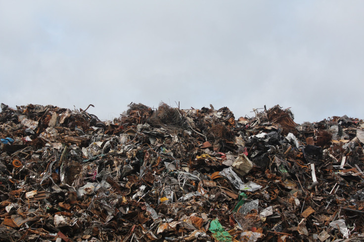
One sector where we can see major methane mitigation is in the materials used to make up our favorite electronics and devices, like phones, tablets and laptops. The components that make up our devices result in a massive amount of electronic waste (E-waste), which is a major contributor to methane emissions. Today, most electronics are made from silicon and thus are not easily recyclable. Also, because silicon is an extremely poor conductor of heat, it requires tremendous cooling, which means our electronic devices require plastic cooling fans and complex packaging materials. Because of silicon’s inefficiencies, when the life of our electronics comes to an end, they either end up in the landfill, which we already know is a huge methane emitter, or are incinerated, which also releases greenhouse gases into the atmosphere.
E-waste is currently the most rapidly growing waste problem in the world, with 50 million tons of it amassing with each passing year.
So, what can be done?
Electrical component manufacturers need to make a committed pivot to the usage of a more sustainable material in the production of electronics, like laptops, cellphones and others. Plain and simple: the only way toward a cleaner atmosphere is through the use of cleaner materials.
The solution lies in advanced materials: materials that have been engineered to outperform conventional ones, like silicon. They are typically harder, more durable and tougher than conventional materials, among other advantageous attributes.
Additionally, advanced materials can replace rare earth metals as thermal materials in electronics. This means that when electronics end up discarded, much of it is simply carbon, which is a material that occurs naturally, as opposed to heavy metals that seep into the earth or pollutants that enter the atmosphere.
Advanced materials, such as lab-grown diamonds, are being rapidly developed, as they have the chance to be the future of the industry. From their creation, all the way to the end of a piece of electronics’ life, advanced materials remain a more environmentally friendly material.
Through a process known as “chemical vapor deposition,” methane is used as the source material to create lab-grown diamonds, which means, right off the bat, diamond takes a greenhouse gas out of the atmosphere. In this instance the very problem we are looking to combat has helped create the solution.
The advantages of advanced materials over silicon do not end with sustainability. Advanced materials not only help with sustainability but also lead to higher efficiency.
As mentioned earlier, advanced materials are thinner and leaner than other, traditional materials, leading to a smaller form factor, finally resulting in electronic products that aren’t nearly as large and bulky, so they can run more efficiently.
Beyond sustainability concerns, perhaps one of the greatest advantages to the use of diamond and other advanced materials is the fact that they run cooler and thinner than current silicon systems. Diamond’s ability to handle more extreme temperatures and higher electrical voltages also lead to more energy efficient electronic devices as well, as they are unbothered by these extremes and can continue to perform with optimal efficiency. These advantages make them not only the most obvious choice for technological advancement but also the obvious choice to combat rising methane emissions from E-waste.
The rise in methane emissions is one of the most devastating issues facing our environment and it is getting worse and will continue to do so if major changes are not made. When it comes to E-waste and electronics, replacing a material, like silicon, with something more sustainable, like diamond, is not only an incredibly effective way of reducing methane emissions but also a very practical one. Lab-grown diamonds and other advanced materials are already being rapidly produced and can be applied to technology in a multitude of ways. This solution not only benefits the environment but also brings the tech industry a step forward into the use of more efficient advanced materials, which will allow the nation to compete in the tech world on a global stage.
(Adam Khan is the founder of AKHAN Semiconductor)
© Copyright IBTimes 2025. All rights reserved.
- MOST POPULAR IN Opinion